
Design Review: LattePanda Mu NAS Carrier
It is a good day for design review! Today’s board is the MuBook, a Lattepanda Mu SoM (System-on-Module) carrier from [LtBrain], optimized for a NAS with 4 SATA and 2 NVMe ports. It is cheap to manufacture and put together, the changes are non-extensive but do make the board easier to assemble, and, it results in a decent footprint x86 NAS board you can even order assembled at somewhere like JLCPCB.
This board is based on the Lite Carrier KiCad project that the LattePanda team open-sourced to promote their Mu boards. I enjoy seeing people start their project from a known-working open-source design – they can save themselves lots of work, avoid reinventing the wheel and whole categories of mistakes, and they can learn a bunch of design techniques/tips through osmosis, too. This is a large part of why I argue everyone should open-source their projects to the highest extent possible, and why I try my best to open-source all the PCBs I design.
Let’s get into it! The board’s on GitHub as linked, already containing the latest changes.
Git’ting Better
I found the very first review item when downloading the repo onto my computer. It took a surprising amount of time, which led me to believe the repo contains a fair bit of binary files – something quite counterproductive to keep in Git. My first guess was that the repo had no .gitignore for KiCad, and indeed – it had the backups/ directory with a heap of hefty .zips, as well as a fair bit of stuff like gerbers and footprint/symbol cache files. I checked in with [LtBrain] that these won’t be an issue to delete, and then added a .gitignore from the Blepis project.
This won’t make the repo easier to check out in the future, sadly – the hefty auto-generated files are still in the repo history. However, at least it won’t grow further as KiCad puts new archives into the backups/ directory, and, it’s good to keep .gitignore files in your KiCad repos so you can easily steal them every time you start a new project.
Apart from that, a .gitignore also makes working with your repository way way easier! When seeing changes overview in git status or GitHub Desktop, it’s way nicer to, and you even get a shot at reviewing changes in your commits to make sure you’re not adding something you don’t want in the repository. Oh, and, you don’t risk leaking your personal details as much, since things like auto-generated KiCad lockfiles will sometimes contain your computer name or your user name.
Now that the PCB Git-ability has been improved, let’s take a look at the board, first and foremost; the schematic changes here are fairly minimal, and already reviewed by someone else.
Cheap With Few Compromises
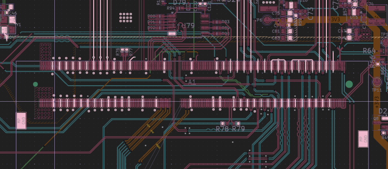
There’s plenty of PCIe, USB3, and SATA on this board – as such, it has to be at least four layers, and this one is. The SIG-GND-GND-SIG arrangement is only slightly compromised by a VDC (12 V to 15 V) polygon on one of the layers, taking up about 30% of space, and used to provide input power to Mu and also onboard 3.3 V and 5 V regulators.
Of course, with so many interfaces, you’ll also want to go small – you’ll have to fit a lot of diffpairs on the board, and you don’t want them flowing too close to each other to avoid interference. This board uses approximately 0.1 mm / 0.1 mm clearances, which, thankfully, work well enough for JLCPCB – the diffpairs didn’t even need to be redrawn much. Apart from that, the original design used 0.4 mm / 0.2 mm vias. Problem? JLC has a $30 surcharge for such vias for a board of this size. No such thing for 0.4 mm / 0.3 mm vias, surprisingly, even though the annular ring is way smaller.
I went and changed all 0.4 mm / 0.2 mm vias to 0.4 mm / 0.3mm vias, and that went surprisingly well – no extra DRC errors. The hole-to-copper distance is set to be pretty low in this project, to 0.15 mm, because that’s inherited from LattePanda carrier files, so I do hope that JLC doesn’t balk at those vias during the pre-production review. Speaking of DRC, I also set all courtyard errors to “ignore” – not only does this category have low signal-to-noise ratio, the LattePanda module courtyard also would raise problems at all items placed under the module, even though there’s plenty of space as long as you use a DDR socket tall enough.
One thing looked somewhat critical to me, though – the VDC polygon, specifically, the way it deprived quite a few diffpairs from GND under them.
Redraw, Nudge, Compromise
Remember, you want a ground polygon all along the underside of the differential pair, from start to finish, without interruptions – that ground polygon is where ground return current flows, and it’s also crucial in reaching the right differential pair impedance. The VDC polygon did interrupt a good few pairs, however.
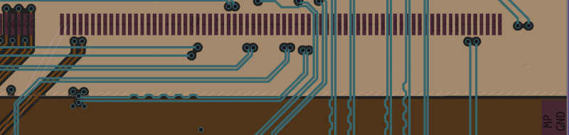
Most of those interruptions were fixed easily by lifting the VDC polygon. Highlighting the net (` keyboard key) showed that there’s only really 4 consumers of the VDC power input, and all of them were above the overwhelming majority of the diffpairs. REFCLKs for M.2 sockets had to be rerouted to go over ground all throughout, though, and I also added a VDC cutout to pull gigabit Ethernet IC PCIe RX/TX pairs over VDC for most of their length.
This polygon carries a fair bit of current, a whole N100 (x86) CPU’s worth and then some, and remember – inner layers are half as thick, only 0. 5oz instead of 1 oz you get for outer layers by default. So, while we can cut into it, the VDC path has to be clear enough. A lot of items on VDC, like some gigabit controller power lines, ended up being moved from the VDC polygon layer to the opposite inner layer – now, they’re technically on the layer under PCIe and gigabit Ethernet pairs, but it’s a better option than compromising VDC power delivery. I also moved some VDC layer tracks to B.Cu and F.Cu; remember, with high-speed stuff you really want to minimize the number of inner layer tracks.
Loose Ends
With the vias changed and polygon redrawn, only a few changes remained. Not all diffpair layer crossings had enough vias next to them, and not all GND pads had vias either – particularly on the Mu and M.2 slots, what’s with high-speed communications and all, you have to make sure that all GND pads have GND vias on them. Again, highlight GND net (`) and go hunting. Afterwards, check whether you broke any polygons on inner layers – I sure did accidentally make a narrow passage on VDC even more narrow with my vias, but it didn’t take much to fix. Remember, it’s rare that extra vias cost you extra, so going wild on them is generally safe.
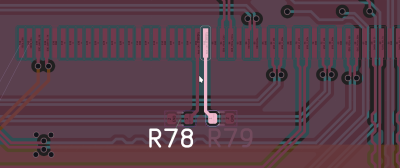
The SATA connector footprint from Digikey was faulty – instead of plated holes for through-hole pins, it had non-plated holes. Not the kind of error I’ve ever seen with easyeda2kicad, gotta say. As an aside, it was quite a struggle to find the proper datasheet on Digikey – I had to open like five different PDFs before I found one with footprint dimension recommendations.
A few nets were NC – as it turned out, mostly because some SATA ports had conflicting names; a few UART testpoints were present in the schematic but not on the board, so I wired them real quick, too. DRC highlighted some unconnected tracks – always worth fixing, so that KiCad can properly small segments into longer tracks, and so that your track moves don’t then result in small track snippets interfering with the entire plan. Last but not least, the BIOS sheet in the schematic was broken for some reason; KiCad said that it was corrupted. Turned out that instead of BIOS.kicad_sch, the file was named bios.kicad_sch – go figure.
Production Imminent
These changes helped [LtBrain] reduce PCB manufacturing cost, removed some potential problems for high-speed signal functioning, and fixed some crucial issues like SATA port mounting pins – pulling an otherwise SMD-pad SATA port off the board is really easy on accident! They’re all on GitHub now, as you’d expect, and you too can benefit from this board now.