Bare Metal STM32: Increasing the System Clock and Running Dhrystone
When you start an STM32 MCU with its default configuration, its CPU will tick along at a leisurely number of cycles on the order of 8 to 16 MHz, using the high-speed internal (HSI) clock source as a safe default to bootstrap from. After this phase, we are free to go wild with the system clock, as well as the various clock sources that are available beyond the HSI.
Increasing the system clock doesn’t just affect the CPU either, but also affects the MCU’s internal buses via its prescalers and with it the peripherals like timers on that bus. Hence it’s essential to understand the clock fabric of the target MCU. This article will focus on the general case of increasing the system clock on an STM32F103 MCU from the default to the maximum rated clock speed using the relevant registers, taking into account aspects like Flash wait states and the APB and AHB prescalers.
Although the Dhrystone benchmark is rather old-fashioned now, it’ll be used to demonstrate the difference that a faster CPU makes, as well as how complex accurately benchmarking is. Plus it’s just interesting to get an idea of how a lowly Cortex-M3 based MCU compares to a once top-of-the line Intel Pentium 90 CPU.
Stitching The Clock Fabric
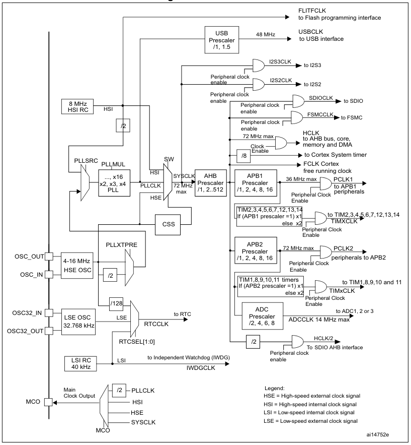
The F103’s clock tree isn’t identical to that of other families of STM32 MCUs, but the basic concepts remain the same. See the below graphic from Reference Manual 0008 for the clock tree of STM32F10x MCUs:
The clock tree of the STM32F10x MCUs. (Source: RM0008)
We can see the HSI clocked at 8 MHz, which feeds into the clock input switch (SW), from where it can provide the 8 MHz system clock without further fuss. Our other options are to use the HSE, which is fed in via its respective oscillator pins and from there is wired to the same switch as the HSI. If we want to get a higher clock speed than what the HSI or HSE can provide directly, we need to use the Phase Locked Loop (PLL) to generate a higher clock speed.
For this we need to first configure the PLL, enable it and select it as the input source for the clock switch. Before we can throw the switch, however, we also need to make sure that the prescalers for the buses (APB1, APB2, AHB) are set correctly. As we can see in the clock tree diagram, we have maximum speeds for each bus and fixed scaling numbers for each prescaler.
This pattern continues with individual peripherals, some of which also have their own prescaler – like USB and the ADC – but this is just something to keep in mind for when using these peripherals. If we’re just trying to crank the CPU core up to its maximum speed and still want to use the UART, all we need is to get the PLL configuration right, along with the AHB and APB prescalers so that the UART peripheral can be interacted with.
Plugging In Numbers
Before we start happily punching numbers on our keyboard to make the MCU go faster, there’s one tedious detail that we have take care of first: appeasing the Flash memory so that it can keep up. This involves configuring the right number of wait states, the use of prefetching and similar options. For this we open our copy of RM0008 to page 60 to ogle at the FLASH_ACR register and its options.
In this Flash access control register for the F103 and kin we get to enable or disable the prefetch buffer and the latency. Fortunately, for the latency the RM tells us exactly how many wait states we have to set here depending on our target system clock speed. For the 72 MHz that the F103 is rated for, we have to set two wait states.
Scrolling up a bit to page 58 and doing the unspeakable thing of reading the documentation, we can see that the prefetch buffer is turned on after reset by default and is best left enabled. As for the half cycle option, this is related to ‘power optimization’, which means that you will not touch this unless you know what you are doing and are sure that you need to change this.
Consequently we can configure our Flash as:
FLASH->ACR |= 2 << FLASH_ACR_LATENCY_Pos | FLASH_ACR_PRFTBE;
Next we wish to use the HSE via the PLL to get the most accurate and fastest system clock speed, which first requires enable the HSE and waiting for RCC_CR_HSERDY to change to 1 as indicate that it is ready for use.
RCC->CR & RCC_CR_HSEON
while ((RCC->CR & RCC_CR_HSERDY) == 0) {
// Handle time-out.
}
Up next is configuring the PLL, starting with setting the PLL source to HSE:
RCC->CFGR |= RCC_CFGR_PLLSRC;
Now we can configure the AHB and APB prescalers. These take the new system clock and divide it by the set number. For the F103, the 36 MHz-limited APB1 needs to be set to 2, while AHB and APB2 can run at the full 72 MHz, ergo 1.
RCC->CFGR |= 1 << RCC_CFGR_HPRE_Pos;
RCC->CFGR |= 2 << RCC_CFGR_PPRE1_Pos;
RCC->CFGR |= 1 << RCC_CFGR_PPRE2_Pos;
Final Steps
Continuing configuring of the PLL and assuming that it is currently disabled, we can now mash in its multiplier number. Unlike other STM32 families, the F1’s PLL is rather simple, with just a single multiplication factor. Since we’re using the HSE, we need to know the board that we are using and the speed that this HSE oscillates at. Taking the common ‘Blue Pill’ STM32F103 board as example, this features an 8 MHz HSE input, meaning that we have to multiply this by 9 to get the target of 72 MHz.
RCC->CFGR |= 7 << RCC_CFGR_PLLMULL_Pos;
The target PLLMUL register starts at 0x02 for a multiplier of x4, ergo we need to subtract two from our target multiplier. With that done we can enable the PLL and wait for it to stabilize:
RCC->CR |= RCC_CR_PLLON;
while (!(RCC->CR & RCC_CR_PLLRDY)) {
// Timeout handling.
}
Next we throw the big switch to use the PLL’s output as the system clock source and wait for the switch to complete:
RCC->CFGR &= ~(RCC_CFGR_SW);
RCC->CFGR |= RCC_CFGR_SW_PLL;
while (!(RCC->CFGR & RCC_CFGR_SWS_PLL)) { }
We should be up and running now, leaving us just to update the global CMSIS SystemCoreClock variable with the new clock speed of 72 MHz.
Benchmarking
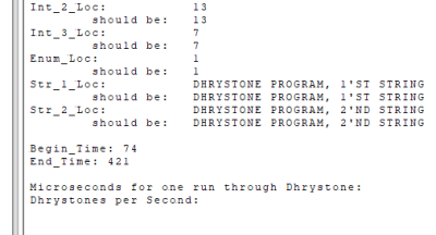
These certainly are Dhrystone results. (Credit: Maya Posch)
Running Dhrystone on our F103 seems like a bit of a challenge as the benchmark was created for your typical desktop and server systems. To achieve this, I took the original pre-ANSI C code for Dhrystone 2.1 and adapted it to a Nodate project. The [url=https://github.com/MayaPosch/Nodate/blob/master/examples/stm32/dhrystone/src/dhrystone.cpp]dhrystone.cpp[/url] file contains the benchmark itself, with no significant modifications other than to set up the MCU and the UART as standard output target. The number of runs is also hardcoded to be 100 million so that it doesn’t have to be punched in every time.
After compiling the benchmark and flashing it to the STM32F103 board, it seemed to take a few eternities for it to complete with so many runs. When the board’s single LED finally started doing its leisurely blinking routine to indicate completion, it turned out that 347 seconds had expired, or roughly 5.78 minutes. As can be seen in the start time, this wasn’t the first attempt, after a 10 million run completed too quickly according to the benchmark’s criteria. C’est la vie.
Annoyingly, the printf-lite implementation that I use with Nodate didn’t seem to like the 32-bit float values and were absent in the final output, so I had to do the calculations for the Dhrystones Per Second (DPS) and related MIPS (DPS / 1757) myself. Since the times() implementation’s ticks equal seconds, this was at least fairly easily, giving the following numbers:
- DPS: ~288,184.438
- MIPS: ~164.021
To see whether these numbers are at all plausible, I consulted a few lists of Dhrystone benchmark results, including one for DPS and one for MIPS. Taking into account the noise created by running it on an OS versus bare metal, my use of -Og optimization level and other differences, the placement at the level of about a Pentium 100 doesn’t seem too farfetched.
There is an official ARM Dhrystone benchmarking guide (AN273), which cites a DPS of 40,600.9 for a Cortex-M MCU running at 18.5 MHz. This would be 158,014 DPS if extrapolated linearly, but obviously not the exact board, MCU or compile flags are used, so ‘rough ballpark’ seems to be the term of the day here.
Perhaps the most interesting finding is that a lowly STM32F103 MCU can keep up with a once high-end Pentium CPU of the early 1990s, at least within the limited integer-only Dhrystone benchmark. Next target will probably be to run the more modern and extensive CoreMark on the F103 and other STM32 MCUs, to give a more holistic perspective.
hackaday.com/2025/12/18/bare-m…