Using 3D Printing and Copper Tape to Make PCBs
In a recent video [QWZ Labs] demonstrates an interesting technique to use 3D printing to make creating custom PCBs rather straightforward even if all you have is a 3D printer and a roll of copper tape.
The PCB itself is designed as usual in KiCad or equivalent EDA program, after which it is exported as a 3D model. This model is then loaded into a CAD program – here Autodesk Fusion – which is used to extrude the traces by 0.6 mm before passing the resulting model to the 3D printer’s slicer.
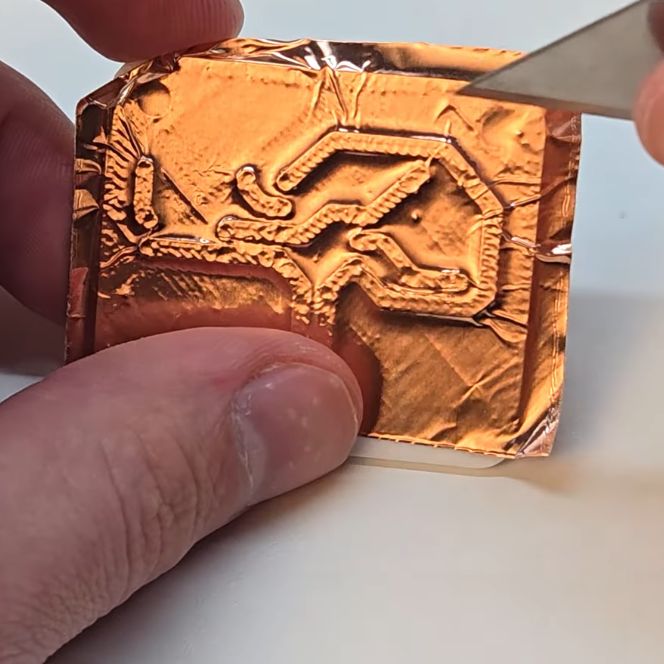
By extruding the traces, you can subsequently put copper tape onto the printed PCB and use a cutting tool of your choice to trace these raised lines. After removing the rest of the copper foil, you are left with copper traces that you can poke holes in for the components and subsequently solder onto.
As far as compromises go, these are obviously single-sided boards, but you could probably extend this technique to make double-sided ones if you’re feeling adventurous. In the EDA you want to use fairly thick, 2 mm trace width with plenty of clearance to make your copper cutting easy, while in the slicer you have to check that the traces get printed properly. Using the Arachne wall generator option for example helps to fill in unpleasant voids, and the through-holes ought to be about 1 mm at least lest the slicer decides that you really want to drill them out later by hand instead.
While soldering is pretty easy on copper tape like this, desoldering would be more challenging, especially with hot air. In the video PLA was used for the PCB, which of course is rather flexible and both softens and melts easily when exposed to heat, neither of which make it look very good compared to FR4 or even FR1 PCB materials. Of course, you are free to experiment with whatever FDM, SLA or even SLS materials you fancy that would work better for the board in question.
Although obviously not a one-size-fits-all solution for custom PCBs, it definitely looks a lot easier than suffering through the much-maligned prototype perfboards that do not fit half the components and make routing traces hell. Now all we need is the ability to use e.g. targeted vapor-deposition of copper to make fully 3D printed PCBs and this method becomes even easier.
youtube.com/embed/PLliKgzKKUI?…
hackaday.com/2026/01/28/using-…